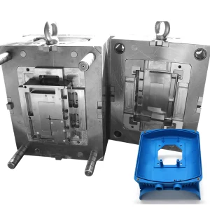
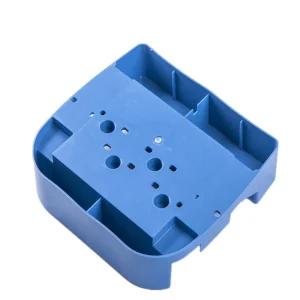
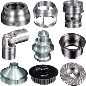
Ningbo Gemnexa CNC Co., Ltd. stands as a premier powerhouse in the domain of precision engineering and mould tooling. Operating from the industrial vanguard of Ningbo, Zhejiang Province, our manufacturing facilities integrate state-of-the-art CNC milling, turning, drilling, and multi-axis machining capabilities. By positioning ourselves at the intersection of material science and mechanical engineering, we deliver components that satisfy the demanding tolerances of the semiconductor, aerospace, medical equipment, and automotive electronics sectors.
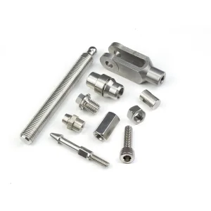
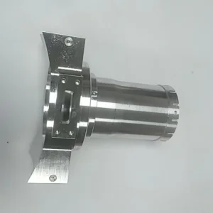
In the contemporary semiconductor industry, where technological iterations are defined by nanometer nodes and sub-micron geometries, the integrity of the process chamber components determines structural yield and overall operational efficacy. Gemnexa CNC works in tandem with leading global fabless houses, original equipment manufacturers (OEMs), and integrated device manufacturers (IDMs). From complex gas distribution plates (showerheads) and electrostatic chuck components to structural vacuum housings, our engineers enforce an uncompromising commitment to dimensional accuracy and surface cleanliness.
Ningbo's world-class deep-water port and robust metalworking supply ecosystem enable Gemnexa CNC to source ultra-pure raw materials and dispatch finished assemblies rapidly. This infrastructure minimizes logistics lead times, ensuring global semiconductor lines and advanced engineering enterprises remain active and operational without bottlenecking delays.
Ultra-Precision Machining Tolerance
Excellent Controlled Roughness Range
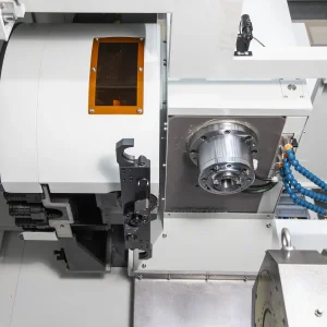
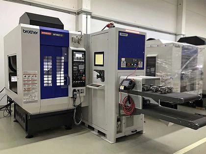
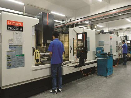
Simultaneous High-Speed Machining Centers
CMM Metrology & Traceability Inspection
The manufacturing environment of semiconductor processes—encompassing chemical vapor deposition (CVD), physical vapor deposition (PVD), atomic layer deposition (ALD), and plasma etching—is chemically hostile. It demands mechanical components that resist high thermal expansion, particle generation, and chemical corrosion from halogen-based plasma gases. Selecting and machining the right materials is the primary challenge in this segment:
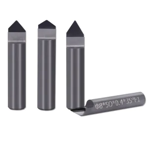
Machining engineering plastics like PEEK, Teflon (PTFE), and Vespel requires tooling configured to avoid mechanical stress and deformation. For high-temperature zones, ceramics such as Alumina (Al2O3), Aluminum Nitride (AlN), and Silicon Carbide (SiC) are ground to absolute dimensional parameters.
Titanium alloys, Kovar, Inconel, and high-purity Aluminum (such as Al6061-T6) are frequently specified for physical vapor deposition steps. Crucially, these metals require passivation and strict surface finish optimizations to prevent heavy-metal contamination of the wafer substrate.
Micro-features in showerheads demand thousands of micro-holes with strict concentricity constraints. Any burr, microscopic deviation, or internal tool mark could disrupt laminar gas flow, yielding uneven thin-film thickness across the processing wafer.
At Gemnexa CNC, we understand that tool geometry, high-speed spindle configuration, and specialized cooling media must be dynamically matched to the material's physical property profile. For instance, high-speed machining of aluminum parts for vacuum systems must minimize thermal load to eliminate residual internal stresses. These stresses, if unaddressed, can release inside the customer's high-vacuum chamber, leading to physical distortion and critical process drift.
Global semiconductor procurement units operate under volatile demand structures, strict trade regulations, and aggressive time-to-market milestones. Standard wholesale supplier models frequently underperform due to inconsistent manufacturing consistency, inadequate quality reporting, or lack of raw material pedigree certifications. Ningbo Gemnexa CNC overcomes these hurdles through systemic structural solutions:
As the microelectronics industry moves toward sub-2nm nodes and 3D heterogeneous packaging layouts, mechanical support structures must evolve in lockstep. The demand for ultra-flat surfaces is skyrocketing; wafer stages and lithography clamping assemblies now require flatness metrics down to several hundred nanometers. Gemnexa CNC is actively addressing these challenges through continuous investment in next-generation manufacturing technology:
1. Ultra-Precision Metrology Integration: Utilizing coordinate measuring machines (CMM) calibrated to sub-micron accuracy, laser interferometry, and contact-free optical surface profilometry ensures every micro-machined slot, chamfer, and bore aligns with specified parameters.
2. Advanced Deburring & Finish Processing: Utilizing electropolishing, magnetic abrasive finishing, and chemical passivation ensures zero micro-burr presence, lowering the risk of particulate contamination in vacuum chambers.
3. Sustainable Green Manufacturing: By implementing closed-loop cutting fluid recycling, optimization programs to reduce raw metal waste, and high-efficiency multi-axis toolpaths, we align with the eco-friendly corporate social responsibility objectives of modern fab operators.